Resulting from the bulk parameters of PbTe there are two special situations which can be reached by the application of the nipi concept to PbTe:
This strength of the potential modulation does not yet influence the wave functions of the "light " electrons. The wave functions of the "heavy " electrons are already influenced but the coupling between neighbouring periods is still high.
.......................................
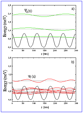
Fig.1a,b: Potential modulation of a periodic series of n- and p- layers with a thickness of dn=dp=30nm and a doping level of NA=ND=1x10^17cm^-3 and wave functions for the light (a) and heavy (b) electrons.
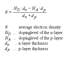
This kind of structures will be used to produce samples with bulk behaviour and very low carrier densities. The main advantage of this technology is that the average carrier density can be controlled by the ratio of the n- and p- layer thicknesses at fixed doping levels:
 ....................................................................................................................................... (1)
The HWE growth of PbTe single layers with low carrier concentrations (n < < 10^17cm^-3) directly by appropriate doping levels is not possible. Low carrier densities (< 2x10^16cm^-3), as an example, are required for experiments concerning the metal-insulator-transition at high magnetic fields and low temperatures. The described technique gives the chance to take up this problem again. Further more a small not vanishing nipi- potential can be used as some kind of adjustable band edge distortion in addition to the native band edge fluctuations.
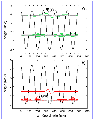
Fig.2a,b: nipi-potential at dn=dp=70nm and ND=NA=1x10^17cm^-3 and wave functions for the light electrons (a) and for the heavy electrons (b).
Fig.2a,b show the same situation as Fig.1 but enlarged single layer thicknesses (70nm single layer thickness and same doping level of 1x10^17cm^-3). The resulting amplitude of the nipi-potential is 4...5 mV. One can see that the wave functions of the light electrons (oblique valleys ) are already modified by the nipi-potential (Fig.2a). From the small splitting of the 5 lowest wave functions one can see that they are only weakly coupled. The reason why there is a set of exactly five such lowest levels results from choosing five nipi-periods for the numerical calculation. Since only the wave functions of the 6 lowest energy levels where plotted there is left only one wave function from the second set of higher subband levels. This subband level lies already nearly "outside" the nipi-potential and therefore it is not localised with respect to the z-direction. Only small perturbations of the periodic nipi-potential will lead to a total de-coupling of the lowest subband states. For example in this numerical simulation (Fig.2a) the period length of the middle nipi-period is accidentally larger by a small amount than the length of the other periods. Even this small deviation leads to a already localised state in this period (lowest energy level in Fig.2a).
But also in real structures one has to deal with a finite number of periods and in the special case of PbTe nipis the boundaries of the periodic nipi-potential are defined by the p-type buffer layers on both the interface to the substrate and at the surface. Therefore in real structures the potential modulation first has to run across the whole energy band gap (ca. 200mV) and after that the nipi-potential starts. Such a structure represents a combination of the potential of a p-n-p structure and a nipi potential which is inserted at the position of the n-layer (Fig.3).
The numerical simulation of the real structure is much more time consuming. For comparison such a numerical calculation is shown in Fig.3.
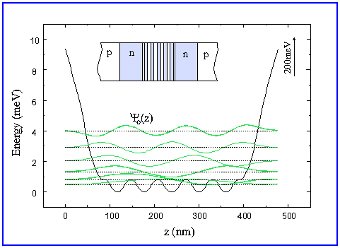
Fig.3: Lower part of the pnp-potential with an inserted nipi-potential including the wave functions of the light
electrons , same layer thicknesses and doping levels as in Fig.1.
Insert: Layer scheme of a real nipi structure
Because of the weak nipi-potential the electrons "feel" the boundaries of the relatively wide pnp-potential (total width: 300nm) more sensitive than the intentional weak nipi-potential. One can see also that the shape of the terminating potential of a real structure has nearly the same effect on the wave functions as the infinite numerical square potential used in the calculation for Fig.1. Therefore the abrupt cut off in the simulations usually is satisfactory conform with real structures. However, if the coupling between the nipi-periods is lifted by any perturbations, the boundaries have no influence on the electronic states anymore.