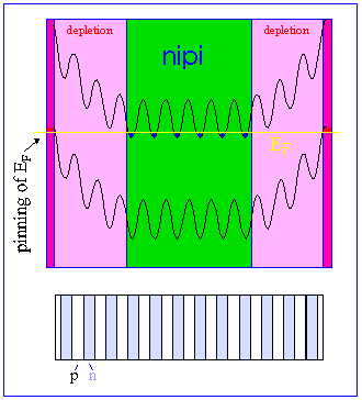
In order to realize a PbTe doping SL, a periodic sequence of alternatively doped layers has to be grown. In the case of ideal compensation, which is difficult to achieve in PbTe where either Te or Pb vacancy states create electrons or holes, no carriers are present. Unfortunately the overall potential scheme depends strongly on boundary conditions and even small deviations from the ideal design parameters may cause drastic changes. In practice, so far mainly BaF2 substrates were used. Since the growth initiates with islands (which merge into another at about 200 nm film thickness) the initial layers show p-type conduction. On the other hand, on the surface of intrinsically doped PbTe a trend towards an accumulation of holes is present. As a consequence of this pinning of the Fermi level on both boundaries an overall potential shape results as indicated schematically in the figure, if the design of the nipi layer is such as to result in n-type conduction. Due to the lack of electrons in the two depleted zones close to the surface and the substrate-interface, the overall band bending is caused by the net positive background charge. If an n-type nipi with relatively small net electron concentration is designed, the length of these depleted zones even increases.