p - i - n - p - structures:
The Hot Wall Epitaxy (HWE), used for the PbTe structures, allows only to produce a sequence of alternatively
doped layers without the ability of growing directly intrinsic layers. The doping of PbTe is achieved either by
resonant vacancy states [6] (Pb vacancies cause p-type and Te vacancies cause n-type conduction) or with extrinsic
doping [7]. Extrinsic doping is done with Tl for p-type and with Bi for n-type conduction.
A alternative way for growing intrinsic layers also with HWE can be the layer scheme suggested in Fig. 3. The
intrinsic zones are achieved by inserting sets of compensated thin sub periods between the main n- and p- layers in
order to approximate the linear potential profile by staircase like small parabolic branches [8].
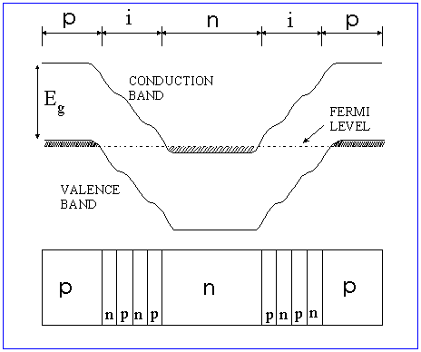
Fig.3: Schematic layer scheme of a p-i-n-i-p structure.
References