p-n-p - structure
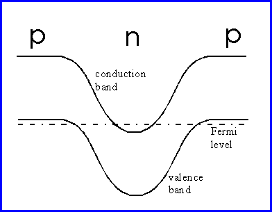
 In order to realize a model structure for a quasi parabolic band edge modulation of the conduction and valence band
a three layer "nipi" offers particular advantages. As shown in the figure the simplest structure which allows the
study of the carrier confinement in parabolic potential consists of one n-type layer embedded in two p-type layers.
Depending on the thickness and on the doping concentrations of the n-type layer either a permanent electron
conduction or a totally depleted n-layer occurs. In order to screen surface effects and to define the position of the
Fermi level on both sides, in the p-type buffer and the top layer, usually a thickness of 0.3 - 0.4 ”m is used i. e.
larger than the depletion length. The apparent disadvantage of this scheme is the following: A variation of potential
modulation by any external influence can immediately result in a loss of the conducting carriers in the n-type layer.
Also a variation of the designed potential is not possible since the modulation always has to be close to the gap
energy. In order to overcome this short coming the shape of the potential between the centre n-type layer and the
buffer- and the top-layer should be varied for a tuning of the properties of that structures. An obvious possibility
would be to introduce intrinsic layers between the n and p layers. Unfortunately PbTe cannot be grown with
concentrations less than 1x10^16cm^-3 either n- or p-type. Another approach consists of a sequence of relatively
thin n- and p-layers which are inserted between the central n-type layer and the two other p-layers which is called a
p-i-n-i-p-structure .
In order to realize a model structure for a quasi parabolic band edge modulation of the conduction and valence band
a three layer "nipi" offers particular advantages. As shown in the figure the simplest structure which allows the
study of the carrier confinement in parabolic potential consists of one n-type layer embedded in two p-type layers.
Depending on the thickness and on the doping concentrations of the n-type layer either a permanent electron
conduction or a totally depleted n-layer occurs. In order to screen surface effects and to define the position of the
Fermi level on both sides, in the p-type buffer and the top layer, usually a thickness of 0.3 - 0.4 ”m is used i. e.
larger than the depletion length. The apparent disadvantage of this scheme is the following: A variation of potential
modulation by any external influence can immediately result in a loss of the conducting carriers in the n-type layer.
Also a variation of the designed potential is not possible since the modulation always has to be close to the gap
energy. In order to overcome this short coming the shape of the potential between the centre n-type layer and the
buffer- and the top-layer should be varied for a tuning of the properties of that structures. An obvious possibility
would be to introduce intrinsic layers between the n and p layers. Unfortunately PbTe cannot be grown with
concentrations less than 1x10^16cm^-3 either n- or p-type. Another approach consists of a sequence of relatively
thin n- and p-layers which are inserted between the central n-type layer and the two other p-layers which is called a
p-i-n-i-p-structure .