Realizing the layer schemes
The problem of depletion layers at the interface to the substrate and at the surface of PbTe n-type layers
(pinning of the Fermi level near the valence band) is a fact which has to be taken into account for the design of the
layer schemes. From this point of view it is not a good way to start immediately the growth with the nipi layer
scheme. If the sheet doping levels are nearly compensated (low free carrier density), no electrons would appear in
the nipi structure and an overall band bending will occur. The reason is that in single layers the depletion zone is
becoming larger if the doping level decreases. In the periodic nipi potential not the doping level of the single layers
is important for this but the average doping level according to Eqn.1 . Since we
aim at low carrier densities (approx. 10% of the bulk doping level) we have to choose an appropriate good
compensation. This leads to larger depletion zones which consists of depleted nipi
periods . Based on the parameters used for the model calculations it turns out that up to 50 nipi-periods can be
depleted. On the other hand an influence of surface and interface states on the electron channel becomes more
dangerous in wide depletion zones if they are beginning immediately at the surface without any screening layers
between.
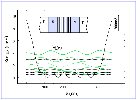
The best way out of this difficulties is to use the layer scheme which consists of a
pnp-structure with the nipi-structure inserted into the n-layer). The thick non depleted p-type buffer layers at the
surface and interface screen influences from the surface and interface states.
The application of this concept is essentially connected to the availability of selective contacts to the buried nipi-
structure.
Of course the design of such structures consisting of doped layers makes short period lengths doubtful because of
the basically statistical distribution of the doping. One has to say that the design parameters of this structures are
approaching the principal limits to some extent. At a doping level of approx. 1.10^17cm^-3 a mean distance
between doping atoms of 20nm results. The typical period lengths for the structures is 140nm. From this numbers
one can expect that the potential fluctuations due to the statistical distribution of the doping is still well below the
amplitude of the nipi potential. A quantitative estimate of the band edge fluctuations gives values around 0.5
mV.
At this point I would like to put foreword again the peculiarities of PbTe. All other materials, which have mainly a
lower dielectric constant, would not allow to reach the proposed limits for the
following reason:
- If the same nipi potential and the same period length is used a much lower doping level would be
necessary. But that is a disadvantage as compared to PbTe because of the statistical distribution of the doping.
- If the amplitude of the nipi potential and the doping level is chosen to be the same as in, the required
period length will be much shorter. This is also not so good because of the doping fluctuations. At the same
time the coupling between neighbouring periods will be high also for the ground states and the transition to
de-coupled periods in a perpendicular magnetic field is not possible.
- At the same doping level and the same period length the amplitude of the potential modulation is getting
to high which is also in contrast to the proposed limits .